Mastering the SMt PCBA Process: An In-Depth Beginner's Guide for Electronics Manufacturing
2025-07-31
Understanding the SMt PCBA Process: A Beginner's Guide
Table of Contents
- What is PCBA?
- Importance of PCBA in Electronics Manufacturing
- Introduction to SMT Technology
- Overview of the SMT PCBA Process
- Step-by-Step Guide to the SMT PCBA Process
- Designing the PCB
- Solder Paste Application
- Component Placement
- Soldering Process
- Testing and Inspection
- Common Challenges in SMT PCBA
- Best Practices for SMT PCBA
- Future of SMT Technology
- Conclusion
- FAQs
What is PCBA?
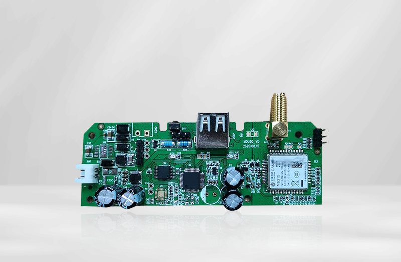
Printed Circuit Board Assembly (PCBA) is the process of assembling electronic components onto a circuit board to create a functional electronic device. This involves soldering components onto a PCB (Printed Circuit Board) through various techniques, including Surface Mount Technology (SMT). Understanding PCBA is crucial for anyone involved in electronics manufacturing, as it forms the backbone of modern electronic device production.
Importance of PCBA in Electronics Manufacturing
The significance of PCBA in electronics manufacturing cannot be overstated. It is the stage where the actual functionality of the electronic device is established. High-quality PCBA ensures that electronic devices operate reliably and efficiently. Moreover, a well-executed assembly process can reduce manufacturing costs and improve time-to-market, giving companies a competitive edge.
Introduction to SMT Technology
Surface Mount Technology (SMT) is a method that allows electronic components to be mounted directly onto the surface of PCBs. This technique is favored due to its ability to accommodate smaller components and improve circuit density. SMT has revolutionized electronics manufacturing, enabling the production of compact and lightweight devices. Understanding SMT is essential for grasping the overall PCBA process.
Overview of the SMT PCBA Process
The SMT PCBA process includes several critical stages, from design to inspection. Each step is integral to producing high-quality assemblies that meet stringent industry standards. The process can be broken down into a series of steps that ensure components are properly placed, soldered, and tested for functionality. Let’s delve deeper into each phase of the SMT PCBA process.
Step-by-Step Guide to the SMT PCBA Process
Designing the PCB
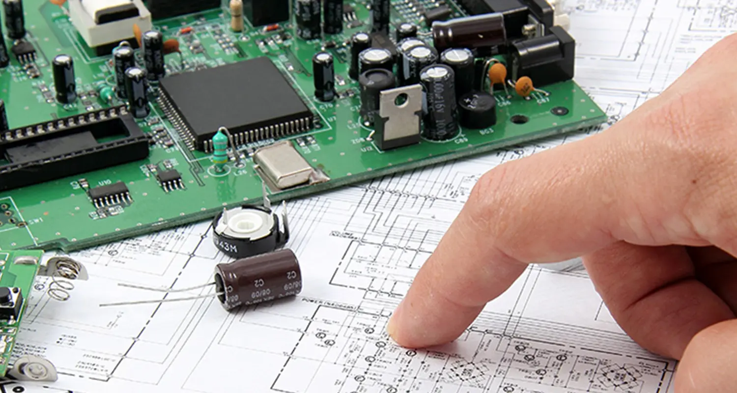
The first step in the SMT PCBA process is the design of the PCB. This crucial phase involves creating a schematic diagram that outlines the electrical connections between components. Designers use specialized software to achieve precision and ensure that the layout is optimized for SMT. Key considerations during this phase include:
- Component placement for optimal space utilization
- Thermal management to prevent overheating
- Signal integrity to maintain performance
Solder Paste Application
Once the PCB design is finalized, the next step is the application of solder paste. This is typically done using a solder paste printer, which applies solder paste to the designated locations on the PCB where components will be placed. The quality of solder paste application is critical, as this influences both the strength and reliability of the solder joints.
Component Placement
After solder paste application, components are placed onto the PCB. This is commonly performed using automated pick-and-place machines that accurately position components on the board. The precision of this stage affects the overall quality of the assembly and its ability to withstand operational stress. High-speed vision systems are often employed to verify component placement and ensure accuracy.
Soldering Process
Once the components are in place, the next step is soldering. This process can be executed in several ways, including:
- Reflow Soldering: The most common method in SMT, where the entire PCB is heated to melt the solder paste, creating strong electrical connections.
- Wave Soldering: Generally used for through-hole components, where the board passes over a wave of molten solder.
- Selective Soldering: A hybrid approach for boards that have both surface mount and through-hole components.
The choice of soldering method depends on the specific requirements of the assembly and the types of components used.
Testing and Inspection
Quality control is a vital step in the SMT PCBA process. After soldering, assemblies undergo rigorous testing and inspection to ensure functionality and reliability. Common testing methods include:
- Automated Optical Inspection (AOI): Uses cameras to detect missing or misaligned components.
- X-ray Inspection: Used for inspecting solder joints, especially in BGA (Ball Grid Array) components.
- Functional Testing: Ensures the completed assembly meets design specifications and performs as intended.
Common Challenges in SMT PCBA
Despite advancements in technology, companies often encounter challenges during the SMT PCBA process. Some common issues include:
- Component Misalignment: Can result in poor solder joints and functional failures.
- Insufficient Solder: Leads to weak electrical connections, potentially compromising device performance.
- Thermal Management Issues: Poor design can lead to overheating of components, impacting longevity and reliability.
Best Practices for SMT PCBA
To overcome challenges and enhance the quality of the SMT PCBA process, adhering to best practices is essential. Some recommended strategies include:
- Invest in High-Quality Equipment: Using advanced machinery and tools can significantly improve accuracy and efficiency.
- Regular Training: Ensuring that personnel are well-trained in the latest techniques and technologies will help maintain high standards.
- Implement a Robust Quality Control Program: Continuous monitoring and testing throughout the process can catch issues early and ensure quality output.
Future of SMT Technology
The future of SMT technology is poised for exciting developments as the demand for smaller and more complex electronic devices continues to grow. Innovations such as AI-driven automation and advanced materials will likely enhance the efficiency and reliability of the SMT PCBA process. Furthermore, the integration of IoT (Internet of Things) technology in manufacturing processes is expected to revolutionize quality control and tracking, making the SMt PCBA process even more efficient and effective.
Conclusion
Understanding the SMT PCBA process is essential for anyone involved in the electronics manufacturing industry. This comprehensive guide provides a clear overview of the key steps, challenges, and best practices associated with the process. By mastering these concepts, individuals can contribute to the production of high-quality electronic devices that meet the demands of the modern market.
FAQs
1. What is the difference between SMT and THT (Through-Hole Technology)?
SMT involves mounting components directly onto the surface of the PCB, while THT requires drilling holes in the PCB to insert components. SMT is generally preferred for modern electronics due to its ability to save space and improve performance.
2. How does automated inspection improve the SMT PCBA process?
Automated inspection systems, such as AOI and X-ray, quickly and accurately identify defects that may be missed by human inspectors. This enhances overall quality control and reduces the risk of faulty products reaching the market.
3. What materials are commonly used in solder paste?
Solder paste typically consists of a mixture of solder alloy and flux. Common solder alloys include tin-lead (SnPb) and lead-free options such as tin-silver-copper (SAC) for compliance with environmental regulations.
4. Why is thermal management important in SMT PCBA?
Effective thermal management ensures that components do not overheat during operation, which can lead to premature failure and reduced lifespan. Proper design and component selection can help mitigate these risks.
5. Can I use SMT for all types of electronic components?
While SMT is versatile and suitable for many components, some larger or specialized components may still require THT. It's essential to evaluate the specific requirements of the design to determine the best approach.
Related News


 WhatsApp
 E-mail